
TokyoMay 21, 2026 /PRNewswire/ — Asahi Kasei Corporation (Headquarters: Chiyoda-ku, Tokyo; Representative Director and President: Koshiro Kudo; hereinafter “the Company”) announced that it has newly developed a “photosensitive polyimide film” (hereinafter “the developed product”) to meet the growing demand for advanced semiconductor packaging for AI semiconductors. The developed product is currently in the customer evaluation phase, with the aim of bringing it to market as soon as possible.

Newly developed photosensitive polyimide film
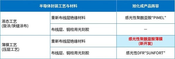
1. Background
The Asahi Kasei Group positions its electronics business as a “key growth” area driving overall group profit growth, and continues to operate electronic materials businesses, including photosensitive polyimide “PIMEL™” and photosensitive dry film (DFR) “SUNFORT™.” Building on these technological foundations, the Company is committed to further advancing materials and process technologies to meet the increasing demands in the advanced semiconductor packaging field.
In recent years, amid the expanding demand for AI data centers, the advanced semiconductor packaging market has seen growing requirements for larger package sizes, such as higher integration of multiple chips and larger interposers. At the same time, the shift from wafer-level to panel-level processes, 3D structuring, and the acceleration of finer and multi-layered packaging substrate wiring have further raised performance demands.
2. Development Overview
The developed product has been created to meet these needs. In addition to leveraging the proven “PIMEL™” technology, it incorporates materials and production techniques accumulated through “SUNFORT™,” which has a strong track record in forming copper pillars essential for fine wiring and 3D packaging, during the film-thinning process. Leveraging these advantages, the developed product can be used not only for redistribution layers in semiconductor packaging but also is expected to be applicable as insulating layers for packaging substrates.
In terms of film processing, the lamination process enables easy formation of uniform insulating resin on large panels, thereby potentially improving production efficiency in semiconductor packaging manufacturing. It also offers excellent film thickness uniformity and is well-suited to handling increased numbers of insulating layers. In the panel-level packaging (PLP※1) field, which is expected to continue expanding, the developed product is anticipated to contribute to improved yield and production efficiency.
Against the backdrop of the increasing scale of advanced semiconductor packaging, research into both liquid and film processes is progressing simultaneously. The Company will continue to develop materials that meet diverse customer needs and actively expand into the market.
Furthermore, the Company is advancing proposals that combine the developed product with the high-performance photosensitive dry film “SUNFORT™ TA Series”※2, capable of forming 1.0μm line-width circuits, to enable both fine wiring and insulating resin layers to be formed through film processes. The Company is also promoting solutions that integrate the photosensitive dry film “SUNFORT™ CX Series,” which can form high-aspect-ratio copper pillars required for 3D semiconductor packaging.

Cross-section of redistribution layer using photosensitive polyimide film and “SUNFORT™ TA Series”
Nobuko Uetake, Executive Officer and Head of Electronic Materials Market Division, Materials Domain, stated:
“As the performance of AI semiconductors continues to improve, advanced semiconductor packaging requires larger-area and higher-precision packaging technologies. Asahi Kasei will integrate the technologies accumulated in photosensitive polyimide resin ‘PIMEL™’ and photosensitive dry film ‘SUNFORT™’ to advance new film process solutions suited to large panels. Through this developed product, we aim to contribute to improving customer yield and production efficiency, while continuing to support the further advancement of advanced semiconductor packaging.”
※1 Panel Level Packaging (PLP): A technology for manufacturing semiconductor packaging using larger panels compared to traditional wafer-level manufacturing.
